You are here
Nanostructuration at the European level
From the microchips in our smartphones to miniature medical analysis devices, micro- and nanostructures are increasingly present in our everyday lives, and there seems to be no end to this trend. Ever smaller transistors, sensors and other intelligent systems are indeed at the heart of considerable innovation and technology transfer issues, particularly in the fields of artificial intelligence and big data. As many countries throughout the world forge ahead in this promising sector, Europe is handicapped by its fragmented academic research in nanomanufacturing and by the absence of coordination among national networks. This issue will be addressed by the EuroNanoLab consortium, which has been set up today by eight European countries and will be coordinated by the CNRS; it already brings together 26 academic clean rooms with a joint investment value of €1.5 billion.
Rapid and continual progress
Since the 1990s, micro- and nanostructures have deeply transformed our environment, often without us being aware of it. Who indeed remembers the first hard drives containing only a few megabytes of memory, which were nonetheless worth a fortune? Today, it only costs a mere hundred euros or so to buy a hard drive with several terabytes and a storage capacity a million times greater, which can hold the contents of a giant library or tens of thousands of hours of music, and is hundreds of times faster than its predecessors. Similarly, everyone now has a smartphone whose calculating capacity exceeds that of the national computing centers of only 30 years ago. In the field of medicine, nanofluidics now makes it possible to perform blood tests with unequalled precision and the CNRS Laboratory for Analysis and Architecture of Systems (LAAS) is working alongside Picometrics-Technologies to develop the BIABooster diagnostic tool that will be able to measure extremely small concentrations of DNA circulating in the blood, and detect the appearance of certain types of cancer in less than 20 minutes.
Whether in the fields of science, artificial intelligence or big data, intelligent systems of the future will be based on breakthrough innovation such as quantum technologies, which will considerably increase the calculation capacity of our processors, make uncrackable encrypted information widely available, and enable the creation of new ultra-high-performance sensors. Atomic-scale transistors, at the highest levels of miniaturization, are also being studied, and in the field of medicine, there are plans to develop nanobiosystems that can be implanted in people, providing real-time monitoring of their health status.
Cutting-edge equipment for nanometric innovations
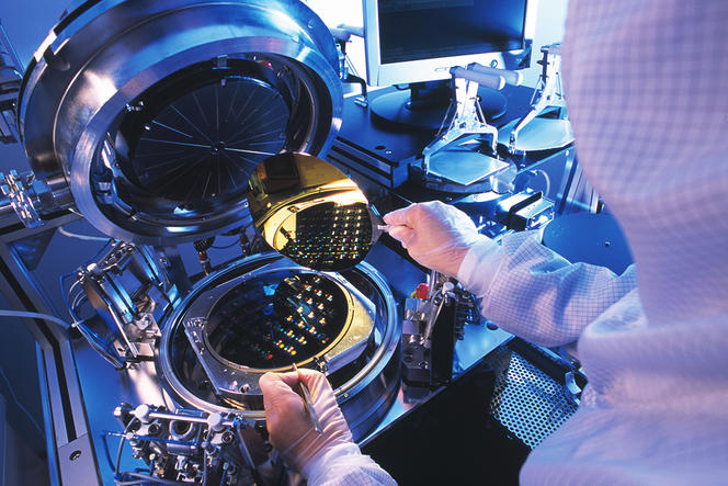
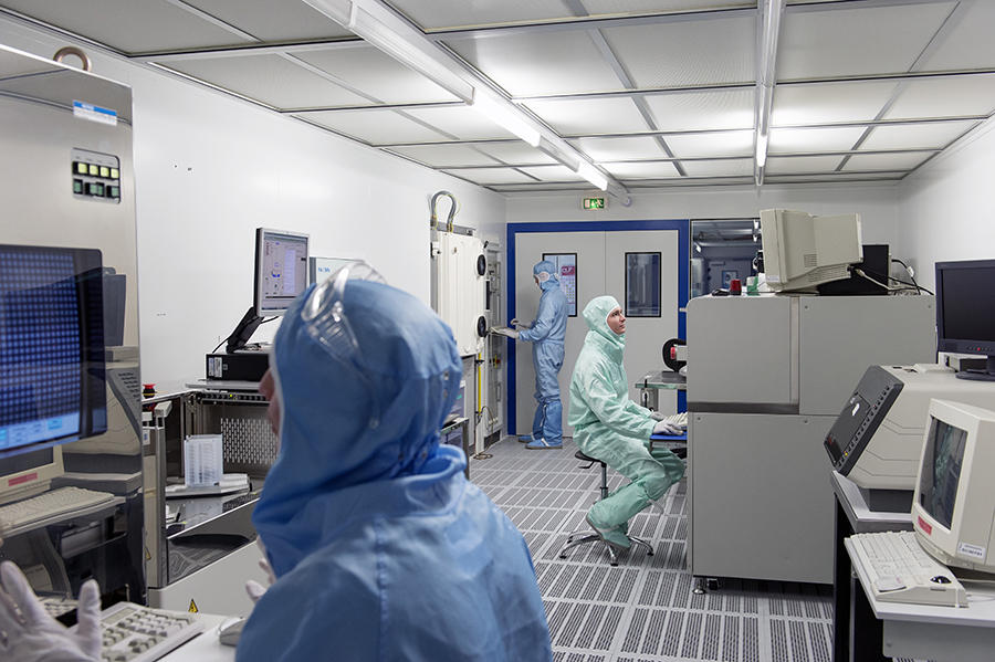
To achieve this, innovative components must be designed, produced and tested, which necessitates extremely advanced nanomanufacturing techniques. These technologies, which require ultraclean rooms and costly equipment, enable the creation of tomorrow’s intelligent information processing systems, with precision at the nanometer level. In view of the considerable stakes involved, most developed countries, in particular the US and Korea, are already investing massively in nanomanufacturing research.
In Europe, the academic players in nanomanufacturing remain highly fragmented, with at least 70 large- or medium-sized centers inside European universities working to develop their expertise without any real coordination between them. Aware of this fragmentation, a number of European countries (Sweden, France, Norway and the Netherlands) have already set up national networks of university clean rooms to promote collaboration at the national level. Today, alongside four other European states (Spain, Portugal, Italy and the Czech Republic), these countries have set up the EuroNanoLab consortium, which already brings together 26 academic clean rooms.

Coordinated research at the European level
To make optimal use of existing investment, EuroNanoLab plans to integrate these academic research facilities around a “central hub” that will monitor them. This new infrastructure will be spread across Europe but will nevertheless be able to develop a common strategy and support such major European projects as the Graphene, Human Brain and Quantum Technologies Flagships, as well as several other important European programs that will no doubt emerge in their wake.
This organization will enable optimal distribution of technological advances between the most suitable nanomanufacturing centers, while ensuring that each of them benefits from their partners’ latest findings. This initiative, coordinated by the CNRS and bringing together a first important group of motivated participants, will be extended to all European countries willing to contribute to it. This new infrastructure, which brings together a large fraction of the community of academic nanomanufacturing centers, will also act as a privileged interlocutor between research and technology organizations (RTO) and their industrial partners. It will ensure effective transfer to industry of the know-how developed by academic centers.
From the pooling of individual skills to the organization of a common European strategy, the development of this nanomanufacturing research network will thus become a hotbed for future technologies destined to become part of our future everyday lives.


