You are here
Graphene Inspires Promising New Materials
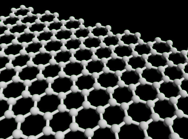
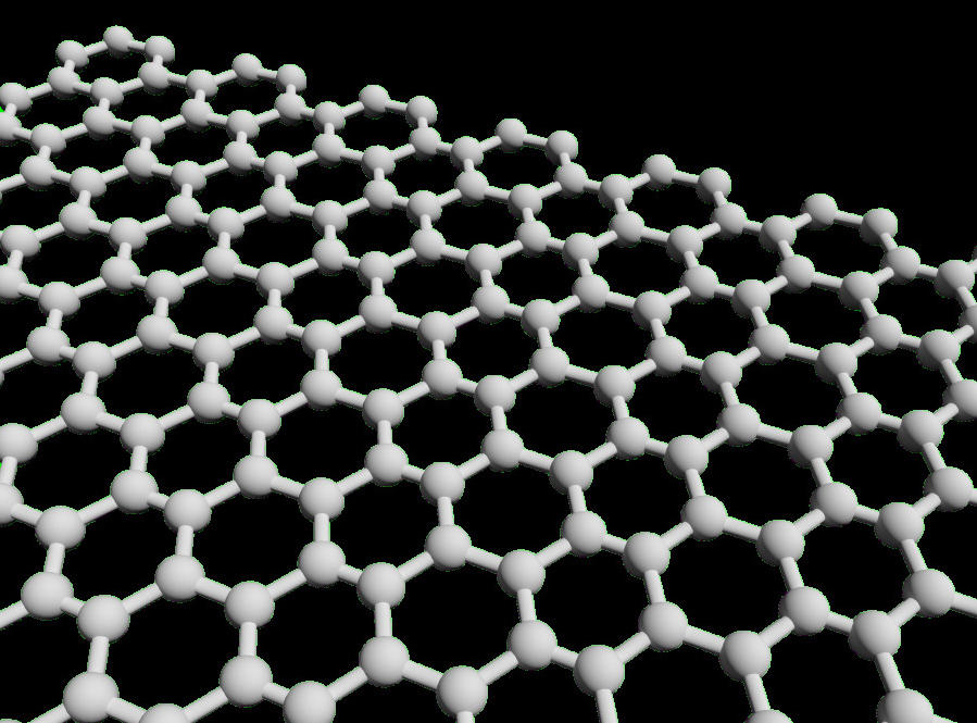
Ultra-flexible, ultra-light, remarkably transparent, stronger than steel, more conductive than copper… The list of qualities that describe graphene, a sheet consisting of a single layer of carbon atoms in a honeycomb lattice, is long and impressive. As soon as this so-called two-dimensional (or 2D) material, the first of its kind, was isolated in 2004, it was heralded as a major breakthrough with myriad applications. In particular, it was expected to revolutionize electronics. Unfortunately, graphene has yet to deliver on its promises in this field. This has not deterred researchers, who are now striving to develop other 2D materials, cousins of graphene that could usher in a new era in electronics.
Semiconductive materials
Although it transports electrons at phenomenal speed, graphene has a drawback: it is not semiconductive, unlike the materials making up the transistors in our computers. Semiconductors carry electricity as soon as their component electrons are subjected to a certain quantity of energy in the form of heat, light or an electric field. This quantity of energy, known as the “band gap,” makes it possible to control the electronic components, “turning them on and off” to create the 0s and 1s at the root of all digital information. But graphene has no band gap, and the efforts made to create one have so far been inconclusive. As a result, “very few people today still believe in the advent of a new age of electronics based on graphene,” reports Guy Le Lay of the Laboratoire Physique des Interactions Ioniques et Moleculaires1 in Marseille (southeastern France).
This lack of progress has encouraged researchers to seek new materials that would be as thin as graphene while offering the advantage of semiconductivity. The stakes are high: such a 2D material would make it possible to reduce the channels that transport electrons, especially in transistors, to the scale of an atom (or nearly so). This would in turn push the frontiers of miniaturization, which is nearing its limits today.
Will silicene spawn a new generation of transistors?
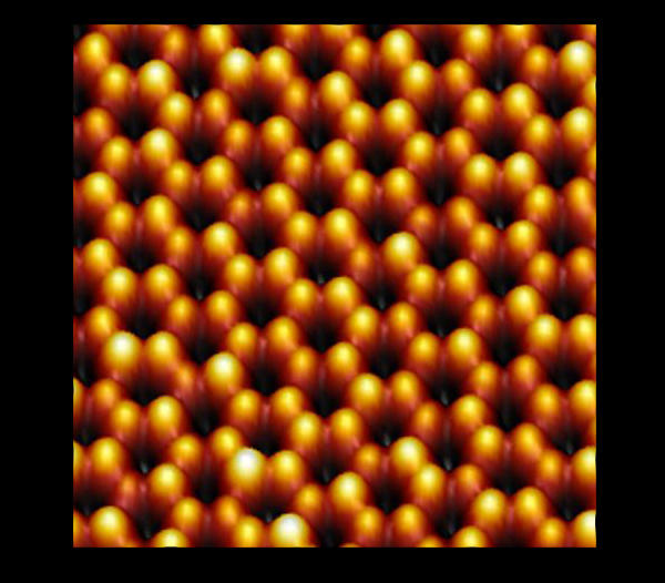
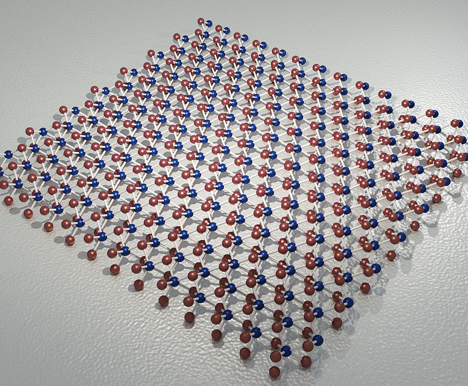
In the 2D materials race, one substance has emerged from the pack: silicene. As its name implies, it is to silicon what graphene is to carbon: a sheet formed of a single layer of silicon atoms, also arranged in a honeycomb pattern. “But unlike graphene, in which all the atoms are on the same plane, the crystal structure of silicene is slightly corrugated,” Le Lay explains. “This characteristic is what makes it semiconductive.” Silicene displays the same high electron mobility as graphene, and another very significant advantage as well: as a derivative of silicon, the basic material of modern electronics, it could easily be integrated into current industrial processes.
Still, silicene is not without its drawbacks. To begin with, it is much more difficult to produce than graphene. Obtaining a sheet of graphene is as simple as using common adhesive tape to peel off graphite, a natural material (used in pencil leads) that is essentially a stack of carbon atom layers. But silicon in its natural state has a different structure from graphite, which means that it must be synthesized artificially.
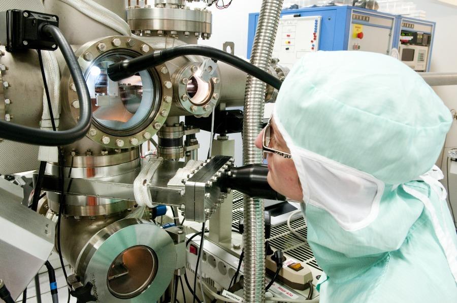
The solution is a process called epitaxy: pure silicon is evaporated in an ultra-high vacuum chamber by bombarding it with an electron beam. The silicon atoms thus released from the block of material are deposited on a substrate whose crystal structure arranges them in a honeycomb configuration. The choice of substrate is crucial. Le Lay’s team, who in 2012 were among the first to synthesize silicene, chose silver. As a metal, however, it is electrically conductive. In an electronic component, the silicene would therefore be inevitably short-circuited by its substrate, becoming useless for practical purposes.

Still, research on silicene is progressing by leaps and bounds. The short-circuit obstacle was bypassed in 2015, when researchers found a way to eliminate the silver substrate and built the first silicene transistor. Others, including a team led by Isabelle Berbezier of the IM2NP2 in Marseille, have been trying to produce silicene on non-metallic substrates. The researcher and her colleagues scored a first this year by successfully synthesizing silicene on the surface of graphene, which "is easy to transfer onto other materials,” Berbezier explains. “The idea is to take advantage of this property to integrate silicene into new-generation transistors.”
Researchers however need to overcome another hurdle before our computers can be equipped with silicene transistors: this extremely reactive material oxidizes very rapidly in the open air. The functional life of the transistor developed in 2015 did not exceed two minutes. Here again, intensive research is underway to extend the material’s lifespan—with encouraging results. Several teams have demonstrated that superimposing multiple layers of silicene protects the lower layers for more than 24 hours. Other strategies are also being tested.
Towards other 2D materials
Silicene, considered the most likely candidate to replace silicon in transistors one day, is not the only contender. Other materials have been synthesized and are now under study, such as germanene, made from germanium atoms, stanene from tin, and phosphorene from phosphorus. It is difficult at this stage to predict which will prove most viable.
Another promising type of material for tomorrow's electronics is transition metal dichalcogenides (TMDs). With a thickness of three atoms, a TMD sheet comprises a monolayer of a transition metal (like molybdenum or tungsten) sandwiched between two layers of sulfur or selenium atoms. TMDs are easy to produce and—as for graphene—adhesive tape is used to peel off a layer from the surface of a natural material consisting of superimposed layers.

This partially explains why these semiconductors have generated more interest than other 2D materials like silicene. In 2011, a team announced the development of the first TMD transistor, using molybdenum disulfide (MoS2). Unfortunately, TMDs have a disadvantage for this application: unlike silicene, their electron mobility is low—to the point that few researchers now believe they will play a role in future transistors.
High potential in optoelectronics
On the other hand, TMDs have many potential applications in optoelectronics, a branch of electronics focusing on devices that can emit or absorb light. In addition to being semiconductive, these ultra-thin materials also interact extremely well with light. “A single sheet of MoS2 can absorb 15% of the light it receives,” notes Xavier Marie of the LPCNO laboratory3 in Toulouse (southwestern France). “That’s ten times the capacity of commonly used materials like gallium arsenide, which are also ten times thicker.” Marie and his team are working on a detailed characterization of the optical properties of several TMDs.
The extraordinary capacity of these new materials can be used to convert light into electricity. When a photon hits the atoms in the crystal, its energy is transferred to an electron that can cross the band gap, thus creating an electric current. Likewise, electricity can be transformed into light by injecting electrons into the TMD sheet.
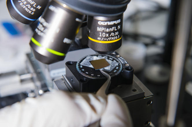
With their remarkable ability to convert light into electricity and vice versa, TMDs are destined to a bright future. They could lead to the development of more sensitive solar cells, miniaturized light sources (LED, laser), or smaller photodetectors, which would be of particular relevance in optical fiber telecommunications. Ultra-flexible like graphene, they could also be used in the display systems of soft screens, a promising sector in which numerous prototypes have already been produced and tested.
While many laboratories continue to develop new 2D materials and look into their properties, others have gone one step further by stacking several of them in superimposed layers. “By combining materials, we hope to be able to benefit from each one’s unique characteristics, or even create materials with completely novel properties,” says Annick Loiseau of the LEM,4 near Paris.
These efforts have already borne fruit. For example, one team has combined MoS2 with graphene to create junctions in solar cells and photodetectors, taking advantage of the semiconductor’s ability to absorb light and graphene’s capacity to transport electrons. The concept has also been applied in the other direction, to create a light-emitting diode using MoS2 placed between two graphene electrodes—and this is just a sampling of the many ideas under investigation.
Yet the fact remains that as of today, devices using 2D materials exist only in the laboratory. To bring them into use, researchers need to get around another key problem, namely their mass production. “For the moment, the production of all these new 2D materials is like haute couture tailoring,” Loiseau emphasizes. “We are not yet able to produce or manipulate them on large surfaces, which is essential if they are ever to find practical applications in electronics.” The researchers are well aware of the issue, and striving to solve it. The history of graphene and its successors has only just begun.
- 1. CNRS / Université d’Aix-Marseille.
- 2. Institut des Matériaux, de Microélectronique et des Nanosciences de Provence (CNRS / Aix-Marseille Université / Université de Toulon).
- 3. Laboratoire de Physique et Chimie des Nano-objets (CNRS / INSA Toulouse / Université Toulouse III Paul Sabatier).
- 4. Laboratoire de l’Étude des Microstructures (CNRS / Onera).


